Electronics
Our solutions for data centers
From infrastructure and power supply to advanced cooling systems, Arkema supports the design of reliable and energy-efficient data centers.
Listen to the podcast: Building the Data Centers of Tomorrow
AI is reshaping data center requirements. Nicolas Champagne explains how advanced materials are enabling higher performance, greater safety and improved sustainability.
Our materials for electronic devices
Reliable solutions for smart devices
Arkema materials are used in a wide range of wearable and consumer electronics, including smart devices designed for everyday use. Advanced polymers enable precise touch control and flexible, durable components, while specialized adhesives ensure reliable assembly and long-term performance. Together, these solutions support more robust, responsive, and sustainable electronic devices.
Rilsan® Clear transparent polyamides, for electronic devices or kitchen robots
Arkema delivers high-performance, bio-based transparent polyamides through our Rilsan® Clear range. With grades up to 60% bio-based content, this range can help reduce carbon footprint while bringing incredible durability and fatigue and chemical resistance. In addition to high clarity, the elevated Tg (glass-transition temperature) of this range allows for consistent performance at elevated tempertures often seen in electronic devices. Rilsan® Clear grades are also super lightweight and ductile, which ensures comfort for users especially in wearable applications. The great chemical resistance helps with lotions, skin oils, and other natural substances for wearable applications such as smatphones or headphones. Its resistance to food and cleaner agents makes it ideal for household appliances such as kitchen robots and blenders.
Ultra-light and super rigid polyamides for electronic appliances
100 % bio-based Rilsan® polyamides (from castor oil) are lightweight (grades as low as 0.86g/cm3) and super strong (grades up to 21GPa modulus) for wearable devices like smartwatches, fitness trackers, and Augmented Reality/Virtual Reality headsets and headphones, ensuring comfort and durability. These materials also find applications in internal/external structural components for devices like laptops, smartphones, and accessories like video game headsets, game consoles and controllers. Household appliances like mixers, coffee machines, and dishwashers take great advantage of the strength and chemical resistance of Rilsan® polyamides as well.
Our photocrosslinkable acrylic resins for screen adhesives and protective coatings
Sartomer's UV curable specialty acrylate resins have a wide range of applications in electronics: touch screens on mobile phones and tablets, coatings on smartphone shells and printed circuit boards.
- They are used to manufacture high-performance adhesives for the touch screens of smartphones and tablets, contributing to optimum light diffusion for very high quality image definition. These high added-value acrylates give adhesives key characteristics: durability, prevention of yellowing and excellent flexibility in the case of flexible screens.
- They are aslo used to formulate protective varnishes for the backs and shells of smartphones and tablets. They give the coating abrasion resistance and a unique matt or gloss finish. These resins cure instantly under UV-LED light. The benefits: no solvent emissions and excellent resistance.
Soft or rigid Pebax® elastomers
The Pebax® elastomer range offers a spectrum of softness, flexibility and rigidity levels. They range from 90A to 80D with seamless overmolding with Rilsan® and Rilsan® Clear polyamides. We recently developped the Pebax® Rnew® range of elastomers wich are partially bio-based and provide a personalized soft-touch experience, along with the advantages of chemical resistance and lasting elasticity, depending of grades.
Lithium-ion battery binders & separator coatings
Kynar® PVDF solutions have been used in lithium ion battery technology for many years as electrode binders for active materials. Arkema's continued innovation has led to solutions that are now being used for both anode & cathode binders and separator coatings. Experimental solutions are also under development based upon low VOC waterborne latex technology.
- The Kynar® HSV series electrode binders offer fast dissolution and easy processing, high adhesion with lower loading, reduced swelling in the electrolyte, lower electrode resistivity, and exceptional high voltage stability.
- The Kynar Flex® LBG series separator coatings provide high electrode adhesion in both wet and dry conditions, exceptional high voltage stability, outstanding dimensional stability, controlled crystallinity, and compatibility with nanoceramics for solvent and waterborne technologies.
Adhesives for micro bonding in electronics
Bostik's Born2Bond™ cyanoacrylate, instant engineering adhesives are designed for complex, precise bonding applications in many industrial markets, including electronics. Compared to traditional instant engineering adhesives, which are based on Ethyl Cyanoacrylate technology, these solutions are Methoxyethyl Cyanoacrylate. As a result, they offer the following advantages to address key market needs: -low odor to improve worker safety -low blooming to enhance aesthetics -fast fixture time to streamline manufacturing processes -excellent stability and flexibility to increase product durability.
Moving to silicon-free, organic electronics
Piezotech® electroactive polymers for next electronics
Thanks to the richness of their chemistry and properties, Piezotech® electroactive polymers offer unique possibilities in flexible, printable, thin sensors, actuators, energy harvesting and many other devices.
Piezotech® FC is a range of flexible, thin, printable ferroelectric, piezoelectric and pyroelectric polymers in powder, inks or film forms. They convert mechanical and thermal energy into electrical energy and vice versa. They serve as base materials for high performance, acoustic, ultrasound, force, impact and pressure sensors in medicals, Human-Machine Interfaces, industrial, wearables, Structural Health Monitoring and consumer electronics markets.
In actuators, they are the key materials for innovative Haptics devices, flexible and thin loudspeaker or smart steerable cathethers.
Piezotech® RT is a unique range of relaxor ferroelectric materials with high dielectric, electrostrictive and electrocaloric properties. Thanks to their un-matched dielectric properties they are used emerging applications such as high-k dielectrics in thin films transistors or electrostatic clutches in haptics. With their unique electrocaloric properties, they are the subject of intense research in next generation sustainable solid-state cooling devices.
With its Piezotech® electroactive polymers trange , Arkema and its academic and industrial partners consinuously innovate for next generation of high performnace sustainable electroncis.
Chips, printed circuits and semiconductors
A less harmful process for electroplating
E-Pure MSA® replaces most classical acids used in Sn or Sn/Pb electroplating baths, and frees processes from toxic lead and hazardous fluoborates. With E-Pure MSA®, bath can operate with lower metal content and allows for reduced waste, sludge and fewer residues and effluents. E-Pure MSA® also offers the possibility to recycle electrolytes.
Zenimid™ Polyimide advanced materials
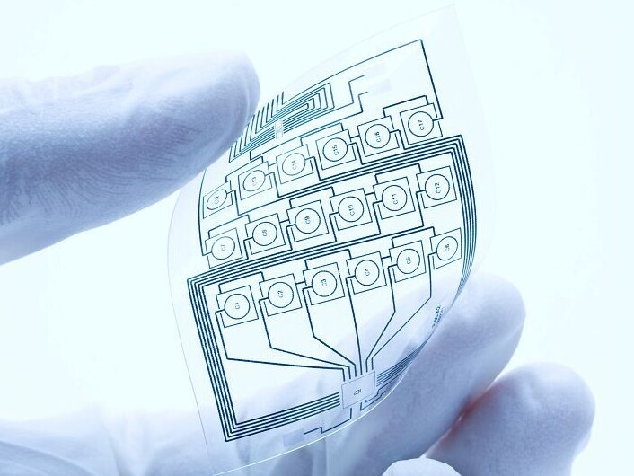
Zenimid™ Polyimide advanced materials deliver exceptional dimensional stability, thermal and electrical properties, making them an ideal choice for the demanding environments of electronics. Their performance profile supports a wide range of advanced applications, from flexible printed circuits (FPCB) requiring flexibility and durability, to heat‑spreading graphite sheets that ensure efficient thermal management in smart devices. Zenimid™ Polyimide advanced materials also enable the high data transfer speed of 5G where their low dielectric constant helps reduce transmission losses and maintain reliable signal integrity. With a combination of outstanding properties, Zenimid™ Polyimide advanced materials enable the continued evolution of crucial components for semiconductors, flexible displays and other next‑generation electronic systems.
MORE ABOUT Zenimid™ Polyimide advanced materials
Foranext® etch gases for electronics
Foranext® etch gases play an important role in the fabrication of semiconductor devices like microchips. Beyond fluorochemical manufacturing capabilities, we add value to the electronic specialty gas suppliers through process control, measurement, and consistency of supply.
Foranext® specialty gases are used to selectively remove material through plasma etching, passivate surfaces to prevent etching, and modify the properties substrates and cleaning chambers.
Our etch gases also allow for the miniaturization of critical features found in memory, logic, microelectromechanical systems (MEMS), and more, which give increased functionality to electronic devices.
Foranext® metrology capabilities for semiconductor manufacturing
Semiconductor device manufacturers demand precise, on-spec ESG composition and Electronic Materials Suppliers (EMS) are under pressure to deliver consistent materials, every time.
Our precision metrology capabilities and laboratory collaborations give EMS competitive advantage in meeting manufacturers’ demands with on-spec material from the start.
Learn more about how our metrology services can help you meet manufacturers contract requirements and waste reduction and sustainability goals.
Our photocrosslinkable acrylic resins for encapsulating printed circuits
Thanks to their dielectric properties, they can be used to protect and encapsulate printed circuit boards, enabling better definition of increasingly smaller printed circuit boards. New formulations are constantly being developed to adapt to this growing miniaturization.
Explore Sartomer solutions
Our cutting-edge amines for electronics
With a legacy spanning six decades, we stand at the forefront of amine manufacturing, employing diverse processes such as alcohol amination and reductive amination of aldehydes and ketones. Our specialized amine multipurpose unit exemplifies adaptability, enabling a wide array of reactions like methylation, cyanoethylation, nitrile hydrogenation, and high-pressure hydrogenation.
Specialized solutions for electronic innovations
In the realm of electronic applications, our alkylamines play a pivotal role in semiconductor manufacturing, facilitating techniques like ALD (Atomic Layer Deposition) and CVD (Chemical Vapor Deposition). These innovations are the backbone of cutting-edge technologies, ensuring precision and reliability in every component.
Driving synthesis excellence
Our amines serve as indispensable synthesis intermediates, enabling the production of:
- Silane Derivatives
- Organometallic Derivatives
Tailored amines for your industry
At the heart of our success lies our dedicated research and development team, committed to define your processes swiftly and effectively. Leveraging our flexible pilot capabilities, we transition seamlessly from concept to commercial volumes.
In the realm of electronic applications, our alkylamines play a pivotal role in semiconductor manufacturing, facilitating techniques like ALD (Atomic Layer Deposition) and CVD (Chemical Vapor Deposition). These innovations are the backbone of cutting-edge technologies, ensuring precision and reliability in every component.
Find out more about our broad range of amines
A multi-product offering for electric cable manufacture
Wide range of polymer solutions for copper and fiber optic cable protection
Cable manufacturers face more stringent requirements in terms of safety (fire resistance), durability (resistance to environmental stresses), while trying to maintain an ease of processing. Our polymers portfolio provides a wide range of solutions to these issues and are used to manufacture various types of copper and fiber optic cables.
- Kynar® and Kynar Flex® polyvinylidene fluoride (PVDF) maintain strong physical characteristics in harsh chemical and thermal settings, making them ideal for demanding applications that need flexibility and toughness. They excel in corrosive, acidic, and high-temperature environments, offering exceptional chemical resistance. Additionally, Kynar® resins provide outstanding abrasion resistance, UV resistance, inherent flame resistance, and minimal smoke generation.
- Our Rilsan® polyamide 11 (PA11), derived from castor oil, is a high-performance polymer with 100% renewable origins, offering valuable properties for the Wire & Cable Industry, including exceptional resistance to short-circuits, mold, fungus, abrasion, termites, rats, chemicals, and a smooth surface finish. PA11 is especially valued in underground electric cables.
Explore Rilsan® polyamide resins
Our specific offering for other industries:
- Agriculture & food industry
- Chemical & plastic industry
- Cooling & refrigeration
- Health, hygiene & beauty
- Mining & metallurgy
- Packaging
- Pulp & paper
- Water management
- Automotive, transportation & aerospace
- Coatings & inks
- Building & construction
- Renewable energy & energy storage
- Adhesives & sealants
- Electrical & electronics
- Oil & gas
- Composites
- Sport & leisure
- 3D printing